(Hong Kong)

Product Summary
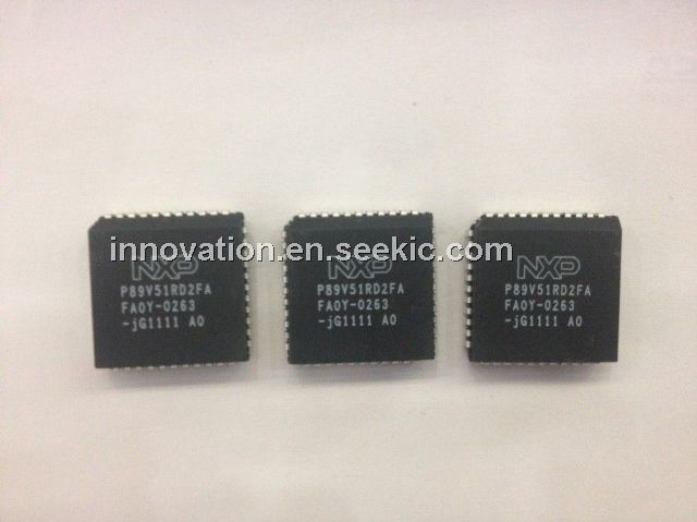
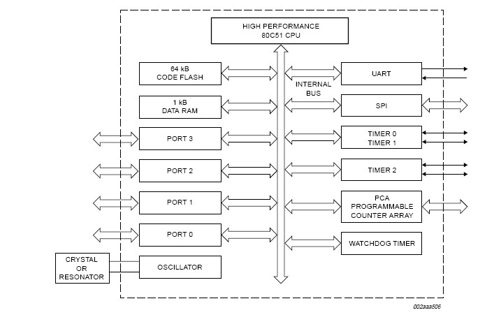
The P89V51RD2FA is an 80C51 microcontroller with 64 kB Flash and 1024 bytes of data RAM. A key feature of the P89V51RD2FA is its X2 mode option. The design engineer can choose to run the application with the conventional 80C51 clock rate (12 clocks per machine cycle) or select the X2 mode (6 clocks per machine cycle) to achieve twice the throughput at the same clock frequency. Another way to benefit from this feature is to keep the same performance by reducing the clock frequency by half, thus dramatically reducing the EMI. The Flash program memory supports both parallel programming and in serial In-System Programming (ISP). Parallel programming mode offers gang-programming at high speed, reducing programming costs and time to market. ISP allows a device to be reprogrammed in the end product under software control. The capability to field/update the application firmware makes a wide range of applications possible. The P89V51RD2FA is also In-Application Programmable (IAP), allowing the Flash program memory to be reconfigured even while the application is running.
Parametrics
P89V51RD2FA absolute maximum ratings: (1)operating bias ambient temperature : -55 to +125 ℃; (2)storage temperature range : -65 to +150 ℃; (3)voltage on EA pin to VSS : -0.5 to 14 V; (4)DC voltage on any pin to ground potential : -0.5 to VDD + 0.5 V; (5)transient voltage (<20 ns) on any other pin to VSS : -1.0 to VDD + 1.0 V; (6)maximum IOL per I/O pins P1.5, P1.6, P1.7 : 20 mA; (7)maximum IOL per I/O for all other pins : 15 mA; (8)total power dissipation per package Tamb = 25 ℃ : 1.5 W; (9)through hole lead soldering temperature 10 seconds : 300 ℃; (10)surface mount lead soldering temperature 3 seconds : 240 ℃; (11)output short circuit current : 50 mA.
Features
P89V51RD2FA features: (1)80C51 Central Processing Unit; (2)5 V Operating voltage from 0 to 40 MHz; (3)64 kB of on-chip Flash program memory with ISP (In-System Programming) and IAP (In-Application Programming); (4)Supports 12-clock (default) or 6-clock mode selection via software or ISP; (5)SPI (Serial Peripheral Interface) and enhanced UART; (6)PCA (Programmable Counter Array) with PWM and Capture/Compare functions; (7)Four 8-bit I/O ports with three high-current Port 1 pins (16 mA each); (8)Three 16-bit timers/counters; (9)Programmable Watchdog timer (WDT); (10)Eight interrupt sources with four priority levels; (11)Second DPTR register; (12)Low EMI mode (ALE inhibit); (13)TTL- and CMOS-compatible logic levels; (14)Brown-out detection; (15)PDIP40, PLCC44 and TQFP44 packages.
Diagrams
| Image | Part No | Mfg | Description |  |
Pricing (USD) |
Quantity | ||||||||||||
|---|---|---|---|---|---|---|---|---|---|---|---|---|---|---|---|---|---|---|
 |
 P89V51RD2FA,512 |
NXP Semiconductors |
8-bit Microcontrollers (MCU) 80C51 64K FL / 1K RM |
Data Sheet |
|
|
||||||||||||
| Image | Part No | Mfg | Description | |
Pricing (USD) |
Quantity | ||||||||||||
 |
P89V51RB2 |
Other |
|
Data Sheet |
Negotiable |
|
||||||||||||
|
P89V51RB2BBC |
NXP Semiconductors |
8-bit Microcontrollers (MCU) 16K/512 FL 12 CLK ISP/IAP COMM |
Data Sheet |
Negotiable |
|
||||||||||||
 |
P89V51RB2BBC,557 |
NXP Semiconductors |
8-bit Microcontrollers (MCU) 16K/512 FL 12 CLK |
Data Sheet |
Negotiable |
|
||||||||||||
 |
P89V51RB2FA,529 |
NXP Semiconductors |
8-bit Microcontrollers (MCU) 80C51 16K FL / 512 R |
Data Sheet |
Negotiable |
|
||||||||||||
 |
P89V51RB2FN,112 |
NXP Semiconductors |
8-bit Microcontrollers (MCU) 80C51 16K FL / 512 R |
Data Sheet |
Negotiable |
|
||||||||||||
|
P89V51RC2 |
Other |
|
Data Sheet |
Negotiable |
|
||||||||||||